Flexible Hybrid Electrics: How Flexible Integrated Circuits Unlock Their Potential
CAMBRIDGE, UK / AGILITYPR.NEWS / May 20, 2020 / Flexible hybrid electronic (FHE) promises to combine the functionality of conventional rigid electronics with the flexibility of printed electronics. A prototypical FHE circuit, in which an integrated circuit is combined with multiple other elements, includes (for example) printed sensors, an antenna, a thin film battery and even thin film PV. Not all components need to be included, or even printed, for a circuit to count as FHE, but it must include as a minimum both printed and placed functionality.
Fundamental to FHE is mounting an integrated circuit (IC), manufactured separately using photolithography, onto a flexible substrate and linking it to printed interconnects. This presents some technological challenges: firstly, silicon dies are rigid, and thus have a completely different form factor and thermal expansion coefficient to the underlying flexible substrate; secondly, alternative semiconductors to silicon, such as metal oxides and organic semiconductors, have much lower mobilities and are difficult to manufacture with sufficiently high yields. These technical challenges and possible solutions, along with other technologies required for FHE circuits, are identified and comprehensively evaluated in the new IDTechEx report: “Flexible Hybrid Electronics 2020-2030: Applications, Challenges, Innovations and Forecasts”.
Packaged ICs: A Temporary Solution
An interim strategy is to solder a conventional packaged rigid IC to a (usually stiffened) flexible substrate. Such circuits are generally referred to as flexible printed circuits (FPCBs) despite having etched interconnects. Unfortunately, mounting a packaged IC substantially impedes flexibility and removes the possibility of R2R manufacturing.
One solution is to use bare dies, a strategy that has been employed for years in RFID tags. These have a very small (< 1 mm2) IC attached at two points using a conductive adhesive to an antenna. However, this application avoids two of the difficulties associated with adding larger, more capable ICs. Firstly, the ICs are so small that their flexibility is almost irrelevant at any realistic bending radius. Secondly, large attachment pads are viable since only two electronic connections are needed.
However, as the ICs become more capable (for example those that incorporate Bluetooth or memory) and hence larger, difficulties begin to arise. Firstly, their lack of flexibility becomes a problem for FHE applications since they cannot conform to the underling substrate.
Flexible ICs From Thinned Si
As such, flexible ICs are beginning to emerge, with the technological approach following 2 divergent paths. The first is to thin existing Si chips by grinding them to just above the first junction. The fragile thin die, with thicknesses as low as 10 um, is encapsulated in a thin layer of polyimide to add fracture protection and make it easier to handle.
This methodology is in principle applicable to many semiconducting chips, with flexible ICs are already available in small volumes for prototyping purposes. This includes a module with Analog-to-Digital-Converter and UHF RFID that measures 2.2 mm by 2.3 mm by 25 um. The current constraint on flexibility is not the die itself but rather the attachment method, which we identify as a key innovation area. Further details are given in the new IDTechEx report: “Flexible Hybrid Electronics 2020-2030: Applications, Challenges, Innovations and Forecasts”.

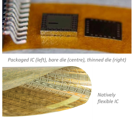
Comparison of packaged, bare and thinned silicon ICs (top, from American Semiconductor), and a wafer sized array of natively flexible ICs (bottom, from PragmatIC). To learn about these innovative technologies more please refer to the new report from IDTechEx: “Flexible Hybrid Electronics 2020-2030: Applications, Challenges, Innovations and Forecasts”.
Natively Flexible ICs From Metal Oxide
The other alternative is natively flexible ICs, at present only available for relatively simple applications such as RFID tags and sensor read-out. While printed ICs have been tried and largely failed, applying the long-established photolithographic techniques to sequentially deposit metal, insulator and metal oxide films on a polyimide substrate has enabled the creation of natively flexible ICs. enabling chips to cost just $0.01.
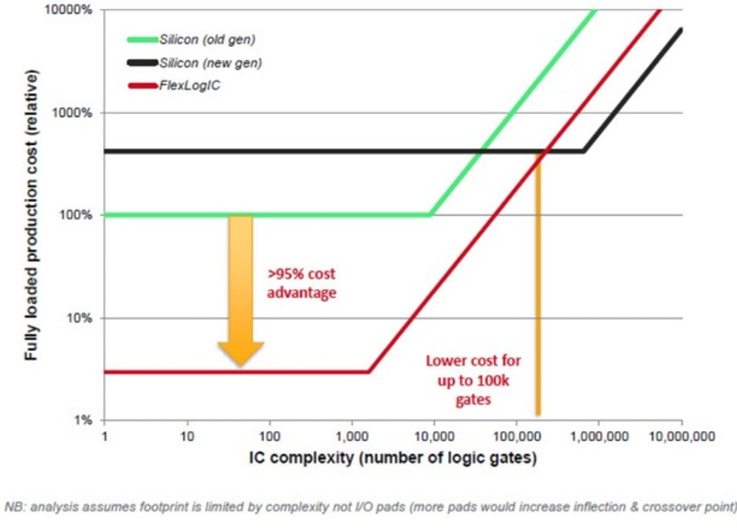
As can be seen from the chart below, natively flexible ICs are cheaper to produce than Si based ICs if there are less than 100,000 logic gates, with the cost for RFID chips around 0.01$. This cost/ complexity characteristic is ideal for applications such as smart packaging, in which low cost rather than processing capability is the limiting factor.

Comparison of total production cost vs number of logic gates for silicon and FlexLogIC chips, which are natively flexible and use a metal oxide as the semiconducting layer (source: PragmatIC). To learn about natively flexible ICs and how they will be employed in FHE circuits, please refer to the new report from IDTechEx: “Flexible Hybrid Electronics 2020-2030: Applications, Challenges, Innovations and Forecasts”.
Flexible IC Adoption
In summary, FHE intrinsically requires alternatives to the rigid packaged ICs used in conventional rigid PCBs and FPCBs. The thinned silicon dies, made more robust by polyimide encapsulation, are likely to find acceptance in applications with more complex processing requirements, such as conventional PCB replacement. Standard bare dies may also be used but require very careful handling to preserve yields. Natively flexible metal-oxide based ICs, currently only capable of HF RFID communication and comparatively straightforward processing of sensor data, will initially be employed in RFID tags and smart packaging applications. Their capabilities, and hence range of suitable applications, is likely to broaden as the technology develops.
A Comprehensive Overview of FHE
Our new report, titled “Flexible Hybrid Electronics 2020-2030: Applications, Challenges, Innovations and Forecasts”, offers a comprehensive analysis of this emerging technology frontier. At IDTechEx we have been assessing and following the printed electronic technologies and markets for well over a decade. This report is based on fresh primary research including interviews and company visits with all the key players worldwide. It identifies and examines all the key innovation trends across the material and production systems, covering attachment, substrate, and metallization materials well as production techniques including high-throughput pick-and-place and various S2S and R2R printing techniques.
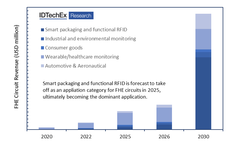
This report builds an application roadmap, showing how FHE will grow in complexity from simple RFID tags of today to complex flexible hybrid electronics of the future, enabling applications in smart packaging, industrial monitoring and wearable devices and more. It offers insightful analysis into application timeline, challenges, and innovation opportunities. Furthermore, it forecasts the growth of this enabling technology, showing that the market can exceed $3 billion by 2030 with the inflection point at which rapid uptake occurs likely arriving in 2025.

Market forecasts for the adoption of FHE for various applications. These forecasts are based on a granular analysis of over 20 sub-categories, the benefits offered by FHE in each category, and price forecasts for application specific components and assembly methods. To learn more please refer to IDTechEx’s report “Flexible Hybrid Electronics 2020-2030: Applications, Challenges, Innovations and Forecasts”.
For more information on this report, please visit www.IDTechEx.com/FlexElec or for the full portfolio of Printed Electronics research available from IDTechEx please visit www.IDTechEx.com/Research/PE.
Join IDTechEx for the new free-to-attend online conference - Opportunities for Printed & Flexible Electronics - on May 27, repeated on May 28. Learn how end-users such as Coca-Cola, Electrolux and Swarovski are progressing printed electronics in their business and hear the latest developments from key suppliers Neotech AMT (manufacturing), Ynvisible (devices) and Roartis (materials). The conference also includes an interactive Q and A session. To find out more and register your place, please visit www.IDTechEx.com/vpe.
About Us
IDTechEx guides your strategic business decisions through its Research, Consultancy and Event products, helping you profit from emerging technologies. For more information on IDTechEx Research and Consultancy, contact research@IDTechEx.com or visit www.IDTechEx.com.
Contacts
Links